今回のあらすじ
SICPの3.3.4 A Simulator for Digital Circuitsを読んでExercise 3.30まで演習問題を解きます。
3.3.4 A Simulator for Digital Circuits
電子回路のシミュレーターを作りましょうという話です。
これまでにやってきた各種データ構造の実装よりはよっぽど具体的で楽しそうですね。
まずは回路を構成する最小要素wireとwireに関するAPIがあるものとして、
それを使って各種回路を表現するところから始めます。
wireそのものの実装と回路のシミュレーターの実装は後回しです。
Exercise 3.28
Define an or-gate as a primitive function box. Your
or-gateconstructor should be similar toand-gate.
これはテキストに載ってる and-gate の実装をちょいと捻れば済むので楽勝ですね:
(define (or-gate a1 a2 output)
  (define (or-action-procedure)
    (let ((new-value
            (logical-or (get-signal a1) (get-signal a2))))
      (after-delay or-gate-delay
                   (lambda ()
                     (set-signal! output new-value)))))
  (add-action! a1 or-action-procedure)
  (add-action! a2 or-action-procedure)
  'ok)

(define (logical-or s1 s2)
  (cond [(and (= s1 0) (= s2 0)) 0]
        [(and (= s1 0) (= s2 1)) 1]
        [(and (= s1 1) (= s2 0)) 1]
        [(and (= s1 1) (= s2 1)) 1]
        [else (error "Invalid signals: " s1 s2)]))
Exercise 3.29
Another way to construct an or-gate is as a compound digital
logic device, built from and-gates and inverters. Define
a procedureor-gatethat accomplishes this. What is the
delay time of theor-gatein terms ofand-gate-delayandinverter-delay?
実装
既存の回路を組み合わせて実装すると言う事は、
コードとしてはテキストに載ってるhalf-adder や full-adder
と似たような形になるはずですね。
後は and-gate と inverter だけで作れるかどうかですね。
これは論理式を適当に変形すれば導けます:
- a ∨ b
- = ¬¬(a ∨ b)
- = ¬(¬a ∧ ¬b)
これを回路図にすると以下の通り:
    ----------------------
    |    na  ___         |
a ----|>o---|   \ nanb   |
    |       |   |-----|>o----- output
b ----|>o---|___/        |
    |    nb              |
    ----------------------
これをコードに翻訳するのは簡単ですね:
    (define (or-gate a b output)
      (let ([na (make-wire)]
            [nb (make-wire)]
            [nanb (make-wire)])
        (inverter a na)
        (inverter b nb)
        (and-gate na nb nanb)
        (inverter nanb output)))
遅延
図から明らかですが、
このor-gateの遅延時間は
(+ (* inverter-delay 2) and-gate-delay)ですね。
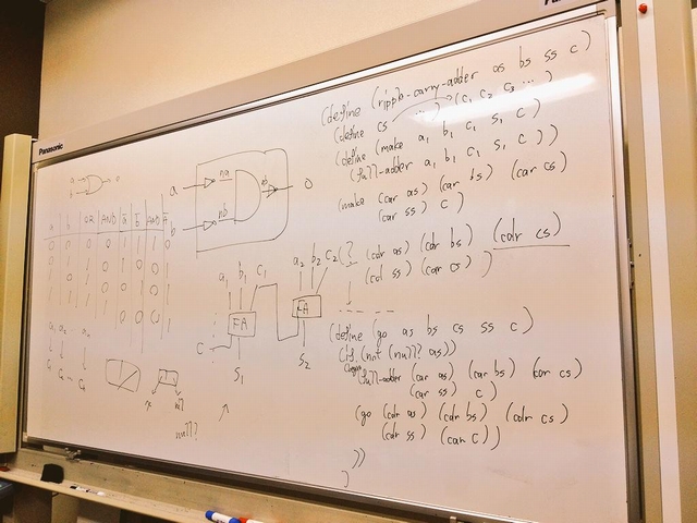
Exercise 3.30
Figure 3.27
shows a ripple-carry adder formed by stringing together
n full-adders. This is the simplest form of parallel adder
for adding two n-bit binary numbers. The inputs A1, A2,
A3, …, An and B1, B2, B3, …, Bn are the two binary
numbers to be added (each Ak and Bk is a 0 or a 1). The
circuit generates S1, S2, S3, …, Sn, the n bits of the
sum, and C, the carry from the addition. Write a procedureripple-carry-adderthat generates this circuit. The
procedure should take as arguments three lists of n wires
each — the Ak, the Bk, and the Sk — and also another wire
C. The major drawback of the ripple-carry adder is the need
to wait for the carry signals to propagate. What is the
delay needed to obtain the complete output from an n-bit
ripple-carry adder, expressed in terms of the delays for
and-gates, or-gates, and inverters?
実装
一見すると図が矢鱈と複雑なので大変そうに見えるのですが、
実際は同じパターンの回路を数珠繋ぎにしているだけです。
となると今まで散々やってきたリスト処理と同じ要領でできますね。
必要なwireのリストを用意して、
それに対して1パターン毎に回路を作っていけばOKです:
    (define (ripple-carry-adder as bs ss c)
      (let go ([as as]
               [bs bs]
               [ss ss]
               [cs (map as (lambda _ (make-wire)))]
               [c-out c])
        (if (not (null? as))
          (begin
            (full-adder (car as) (car bs) (car cs)
                        (car ss) c-out)
            (go (cdr as) (cdr bs) (cdr ss)
                (cdr cs) (car cs))))))
n個のfull-adderを繋ぐ各wire (Figure 3.27におけるC1, C2, C3, …, Cn)を作るところ
(map as (lambda _ (make-wire)))がやや技巧的かも知れません。
n要素のリストは既に引数として受け取っているので、
これを map で「変換」すれば簡単に作れます。
「変換」と言いつつ元のリストの要素は全く使ってないところがポイントで、
ちょっと頭を捻らないと出てこないと思います。
遅延
読み難くなるので各遅延時間の定数を以下のように略記することにしましょう:
- Da = and-gate-delay
- Do = or-gate-delay
- Di = inverter-delay
- Dh = half-adderのdelay
- Df = full-adderのdelay
ripple-carry adderの遅延時間はFigure 3.27から明らかにfull-adderの遅延時間のn倍ですが、
full-adderはhalf-adderを組み合わせて構成されているので、
まずはhalf-adderの遅延時間を確定させる必要があります。
が、Figure 3.25を見れば明らかなようにhalf-adderの遅延時間は2Da+DiかDa+Doのどちらか長い方になります。
これだと各遅延時間の定数の設定によって結果がどうなるか変わってきて面倒臭いですね。
という訳でここではor-gateがExercise 3.29の通りに実装されていると仮定して求めましょう。
そうすると Da + Do = Da + (2Di+Da) = 2Da + 2Di > 2Da + Di ですから
half-adderの遅延時間は 2Da + 2Di だと言えます。
そうするとfull-adderの遅延時間はFigure 3.26から
Df = 2Dh + Do = 2(2Da + 2Di) + (2Di + Da) = 5Da + 6Di
になります。
となるとnビットのripple-carry adderの遅延時間は n Df = n(5Da + 6Di) になりますね。
次回予告
3.3.4 A Simulator for Digital CircuitsのRepresenting wiresから読み始めます。
できればこの節の最後まで進めたいですが、
多分そこまでできなくてExercise 3.31で力尽きるかな……?

#人気の記事
#タグ